Unprecedented single-digit-nanometer magnetic tunnel junction demonstrated

A research group from Tohoku University has revealed ultra-small magnetic tunnel junctions (MTJs) down to a single-digit-nanometer scale that have sufficient retention properties and yet can be switched by a current.
Spin-transfer torque-magnetoresistive random access memory (STT-MRAM) has been intensively developed in recent years and commercialization is expected in 2018. STT-MRAM is capable of replacing existing semiconductor-based working memory due to its excellent capabilities in terms of operation speed and read/write endurance. Moreover, it is nonvolatile, i.e., no power supply is required to retain stored information, making it indispensable for future ultralow-power integrated circuits.
MTJs are the heart of STT-MRAM. To continue the journey to increase the performance and capacity of STT-MRAM, it was essential to make the MTJ smaller, while maintaining the capabilities of retaining information and switching via a small current. CoFeB/MgO-based MTJs developed by the same group in 2010, which used interfacial anisotropy at the CoFeB/MgO interface, paved the way to 20-nm generation. However, below 20-nm, the desirable retention and switching properties could not have been realized simultaneously. Therefore, another approach was required.
![Comparison of relation between thermal stability factor and MTJ diameter for the 'shape-anisotropy' and 'interfacial-anisotropy' MTJs. [1] S. Ikeda et al., Nature Materials 9, 721 (2010). [2] H. Sato et al., Applied Physics Letters 105, 062403 (2014). Credit: Shunsuke Fukami Unprecedented single-digit-nanometer magnetic tunnel junction demonstrated](https://scx1.b-cdn.net/csz/news/800a/2018/4-unprecedente.jpg)
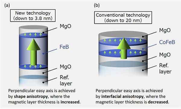
The research group at Tohoku University used a "shape anisotropy" that had not been used effectively in devices suitable for integration, and developed ultra-small MTJs down to less than 10 nm, or a single-digit-nanometer scale.
The shape-anisotropy MTJ has a pillar-shaped magnetic layer by which the film's normal direction becomes a magnetic easy axis (Fig. 1 (a)). This is in contrast to the interfacial-anisotropy MTJs, which were achieved by reducing the thickness of the magnetic layer (Fig. 1 (b)). The smallest diameter of MTJ studied was 3.8 nm, which is an unprecedented scale based on previous research endeavors.
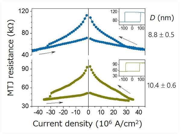
Sufficiently high retention properties, represented by thermal stability factors, were obtained (Fig. 2); the obtained value of more than 80 had never been achieved through the conventional scheme. Furthermore, current-induced magnetization switching is observed for the "shape-anisotropy" MTJs with various diameters including below 10 nm devices (Fig. 3).

The developed MTJ can work with generations of future semiconductor technologies. The single-digit-nanometer MTJ corresponds to more than 100 Giga-bit capacity, which is about 100-times larger than the current working memory technology.
More information: K. Watanabe et al, Shape anisotropy revisited in single-digit nanometer magnetic tunnel junctions, Nature Communications (2018). DOI: 10.1038/s41467-018-03003-7
Journal information: Applied Physics Letters , Nature Communications
Provided by Tohoku University


