October 12, 2018 feature
Nanoscale spin-wave circuits based on engineered reconfigurable spin-textures

Information processing technologies that are typically based on electron charges can also theoretically make use of the electric spin. Magnon spintronics can harness quantized spin waves, magnons, as carriers of spin currents in integrated magnonic circuits. The wave character and joule heating-free propagation of spin waves is a promising combination to engineer highly efficient computing platforms with integrated magnonic circuits. While crucial, the realization of nanoscale circuitry is extremely challenging due to the difficulty of tailoring nanoscopic magnetic properties using existing, conventional techniques. Magnonics is therefore a young field of research at the intersection of the study of spin dynamics and nanoscale science and technology.
In a recent study, now published in Nature Communications Physics, multidisciplinary physicists in the U.S. and Europe collaboratively developed nanoscale, reconfigurable, spin wave circuitry using patterned spin textures. In the work, Edoardo Albisetti and co-workers visualized and channeled the propagating spin waves in arbitrary nanomagnonic waveguides using space and time-resolved scanning transmission X-ray microscopy imaging (STXM), without external magnetic fields or currents. In addition, the physicists demonstrated a prototypical circuit based on two converging nanowaveguides to allow for tunable spatial superposition and interference of confined spin wave modes. The work lays groundwork to use engineered spin textures as building blocks for spin wave based computing devices.
Spin-wave manipulation is a promising alternative to conventional electronics to develop energy-efficient computing platforms, with many concepts proposed in the past few years to realize the concept, from dipole-exchange spin waves in restricted geometry to spin-orbit torque-based spin wave fibers. A major challenge that has hindered the realization of nanoscale spin wave circuits is the efficient channeling and steering of spin waves, thus far only integrated in micron-sized elements via external fields, or by using arrays of nanomagnets. In the path to nanomagnonics, it is highly appealing to consider the use of nanoscale spin textures to control the propagation of spin waves, although conventional methods have hindered such efforts based on domain walls (at which magnetic dipoles or spins reorient themselves). In addition, the capability of steering spin textures to control spin waves in a nanoscale spin wave circuit has also remained elusive. Moreover, the confined dimensions of such spin wave modes are yet to be observed and investigated in detail.

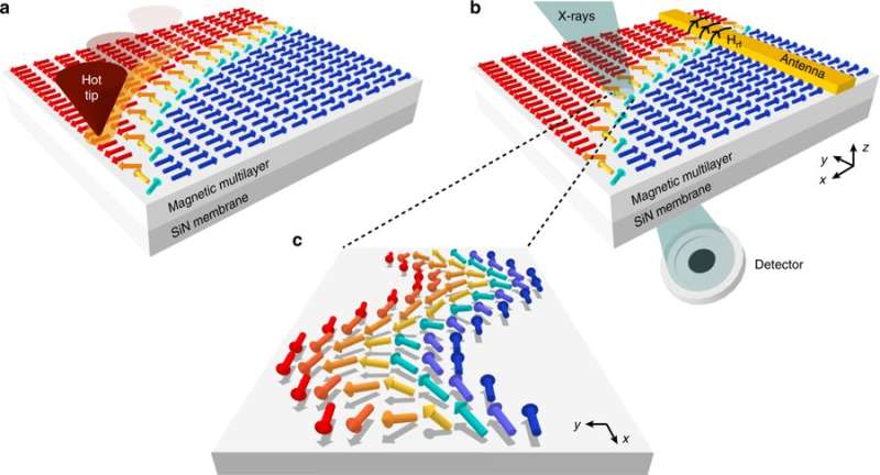
Albesetti et al. demonstrated the fundamental building blocks of spin wave circuitry using arbitrarily shaped magnonic nanowaveguides and prototypic spin wave circuits. The setup allowed the tunable superposition of signals propagating in two converging waveguides by patterning the spin texture of a ferromagnetic thin film using a previously established technique of thermally assisted magnetic scanning probe lithography (tam-SPL). The absence of physical patterning and reversibility of the tam-SPL technique allowed fully reconfigurable nanomagnetic structures based on spin textures with engineered functionality. Direct evidence was provided via observations made using space- and time-resolved STXM on the channeling and steering of localized spin wave modes propagating within straight and curved domain wall-based waveguides, without an external magnetic field.
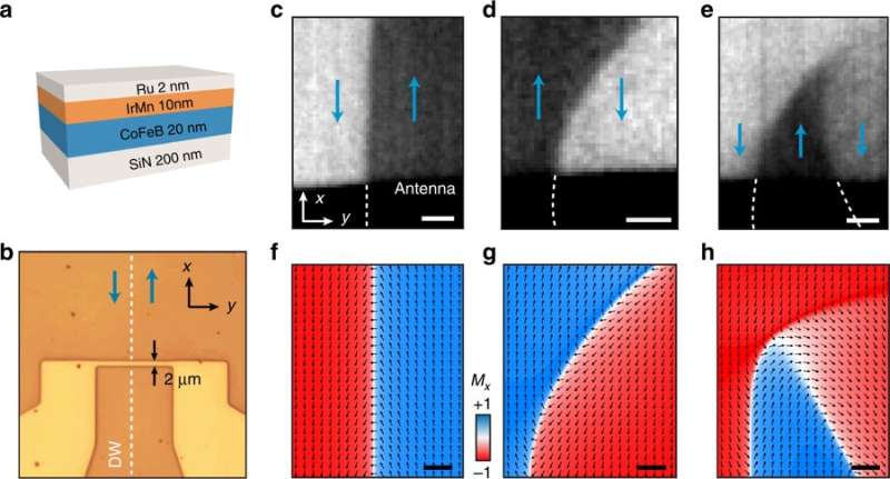
The authors patterned different spin textures in an exchange bias ferromagnetic/antiferromagnetic bilayer by sweeping a heated scanning probe using tam-SPL. The process set the strength and direction of unidirectional magnetic anisotropy in the ferromagnetic film, allowing nanopatterning of engineered spin-configurations. By controlling the geometry of the area scanned by the tip, straight and curved domain walls were obtained. The patterned spin textures and localized spin wave modes were characterized using STXM. A microstrip antenna was employed for the spin wave excitation propagated freely along the wall, in modes known as Winter magnons.
Thereafter, stacks of Co40Fe40B20 (20 nm), Ir22Mn78 (10 nm) and Ru (2 nm) were deposited on 200 nm thick Si3N4 membranes via DC magnetron sputtering by applying a 30 mT magnetic field to fabricate the waveguides. Microstrip antennas (2 µm x 30 µm) were fabricated in the device using optical lithography. The engineered exchange bias multilayer was optically imaged to visualize the orientation of the patterned domain wall with respect to the antenna. Static STXM images displayed spin textures patterned via tam-SPL, followed by corresponding micromagnetic simulations.
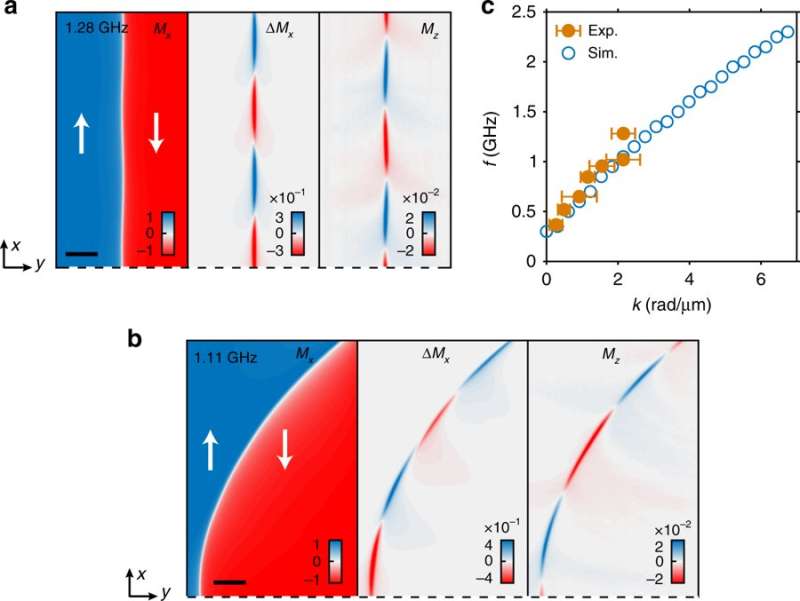
The researchers used time-resolved transmission X-ray microscopy at the polLux (X07DA) endstation of the Swiss Light Source to obtain time-dependent magnetic configuration of the samples. Using the technique, spin waves were imaged stroboscopically with a point resolution between 40 – 75 nm; results for curved and straight walls were reported. Gaussian filtering was used to enhance the contrast with an excitation frequency (1.28 GHz) without an external static magnetic field. The spin waves confined at the domain wall propagated away from the antenna located at the bottom of the panels.
spin waves propagating along a curved path were observed thereafter at an excitation frequency of 1.11 GHz. spin waves were confined at the patterned walls and detected up to 2 µm away from the antenna. The authors also reported on longer propagation distances along a curved domain wall detectable up to 3.5 µm away from the microstrip antenna.
In the study, micromagnetic simulations were carried out by solving the Landua-Lishitz-Gilbert equation of motion integrated within the open-source software MuMax3. The simulations were in good agreement with the experimental results to confirm propagating character of the excitations. Demonstration of the propagating character and the positive dispersion confirmed the possibility to use such guided modes to transport information within integrated nanomagnonic circuits. Waveguides that can control and manipulate confined spin-modes constitute fundamental building blocks to realize nanomagnonic devices. The authors thereafter demonstrated a nanomagnonic circuit that allowed tunable spatial superposition and interference of the guided spin wave modes propagating in two converging waveguides.

Using STXM images the authors showed a spin texture comprising two domain-walls that could be controlled via the application of a small static magnetic field ranging from 2 mT – 1.68 mT. The system was extensively characterized to anticipate the control of the superposition and other properties of the guided modes via external stimuli to envision the implementation of logic functions in spin texture based devices; as previously only projected with the concept of spin wave interferometers.
In this work, the authors engineered a prototypical nanomagnonic circuit that allowed tunable spatial superposition of signals propagating in two converging waveguides. The prospect of developing a reconfigurable nanoscale circuit was a long-standing experimental challenge. The work demonstrated that engineered spin textures were a powerful, versatile tool that allowed experimental development of nanocircuitry. The research marks a fundamental transition in the experimental advancement towards integrated nanomagnonic computing devices.
More information: Edoardo Albisetti et al. Nanoscale spin-wave circuits based on engineered reconfigurable spin-textures, Communications Physics (2018). DOI: 10.1038/s42005-018-0056-x
A. V. Chumak et al. Magnon spintronics, Nature Physics (2015). DOI: 10.1038/nphys3347
E. Albisetti et al. Nanopatterning reconfigurable magnetic landscapes via thermally assisted scanning probe lithography, Nature Nanotechnology (2016). DOI: 10.1038/nnano.2016.25
György Csaba et al. Perspectives of using spin waves for computing and signal processing, Physics Letters A (2017). DOI: 10.1016/j.physleta.2017.02.042
Journal information: Nature Physics , Nature Nanotechnology , Physics Letters A
© 2018 Phys.org


