January 15, 2019 feature
Three-dimensional femtosecond laser nanolithography of crystals
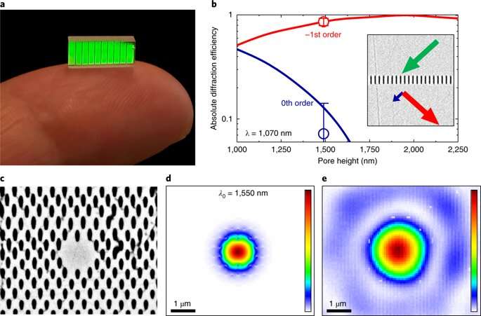
Optical properties of materials are based on their chemistry and the inherent subwavelength architecture, although the latter remains to be characterized in depth. Photonic crystals and metamaterials have proven this by providing access through surface alterations to a new level of light manipulation beyond the known natural optical properties of materials. Yet, in the past three decades of research, technical methods have been unable to reliably nanostructure hard optical crystals beyond the material surface for in-depth optical characterization and related applications.
For example, laser lithography developed by the semiconductor industry is a surface-processing technique used for efficient etching of a range of materials, including silicon, silica glass and polymers. The process can produce high-quality two-dimensional (2-D) nanophotonic devices that can be extended to 3-D, which was demonstrated two decades ago with infrared femtosecond laser direct writing. However, the photopolymerized structures are impractical as they cannot be interfaced with other photonic elements. While 3-D nanostructured optical fibres have delivered functionalities well beyond those possible with ordinary unstructured glass to revolutionize nonlinear optics and optical communications, reliable manufacture of materials in crystalline media has remained elusive.
Alternative methods include direct machining 3-D nanostructures with laser-induced dielectric breakdown and micro-explosions triggered inside transparent crystals to form voids and induce sub-micrometer structures within them. But such methods occurred at the risk of extended lattice damage and crack propagation. Therefore, despite efforts, a standard method for large-scale, 3-D volume crystal nanostructuring remains to be reported.
In a recent study published in Nature Photonics, Airán Ródenas and co-workers at the Institute of Photonics and Nanotechnology and the Department of Physics departed from existing methods of engineering the crystal nanoarchitecture. Instead, they proposed a method whereby the inner chemical reactivity of a crystal, given by its wet etch rate, could be locally modified at the nanoscale to form dense nanopore lattices using multiphoton 3-D laser writing (3DLW). The interdisciplinary scientists showed that centimeter-long empty pore lattices with arbitrary features at the 100 nm scale could be created inside key crystals such as yttrium aluminum garnet (YAG) and sapphire, typically used for practical applications. Ródenas et al. performed direct laser writing before etching, creating the desired pore architecture inside the solid-state laser crystal for photonic applications.
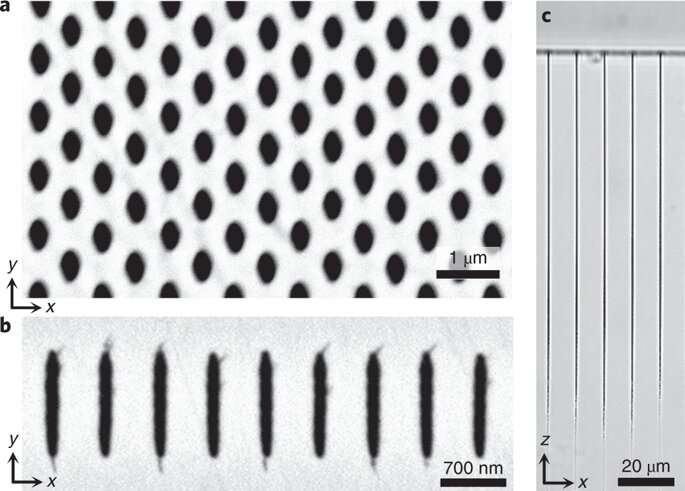
In the experiments, the scientists used a standard 3DLW with an ytterbium mode-locked ultrafast fiber laser (1030 nm wavelength and 350 fs pulse duration). A 1.4 numerical aperture (NA) oil-immersion objective was used to tightly focus the laser pulses inside the crystals. Ródenas et al. used computer-controlled XYZ linear stages for 3-D nanopositioning of the samples. After laser irradiation, they laterally polished the crystals to expose the irradiated structures followed by wet chemical etching. For this, the YAG crystals were etched in hot phosphoric acid in deionized water. A key technical limitation of the etching process was the difficulty in refreshing the exhausted acid inside the nanopores fabricated using the method detailed.
The results showed an etching selectivity at a value larger than 1 x 10⁵ at the molecuar level between the modified and pristine crystalline states, hitherto not observed in a photo-irradiated material. The observed value was approximately two orders of magnitude higher than that of alumina etch masks on silicon. Ródenas et al. determined the etching rate of unmodified YAG at ~1 nm/hour. The proposed method allowed the design and fabrication of nanophotonic elements inside a crystal that could provide the desired optical responses, at the subwavelength structure. The scientists were able to control the features of pore direction, size, shape, filling fraction and length of nanopore lattices in YAG crystals by combining 3DLW and wet etching.
The YAG lattice was etched for 120 hours to obtain average pore dimensions in the x and y directions. The pore shape and size were controlled by tailoring the laser power and polarization. The diameter of etched nanopores depended on the laser power and could be studied for both linear and circular laser beam polarizations. As limitations of the technique, they found that 3-D photonic structures were characteristically isolated in space, needed supporting walls, and suffered shrinkage and a low optical damage threshold.
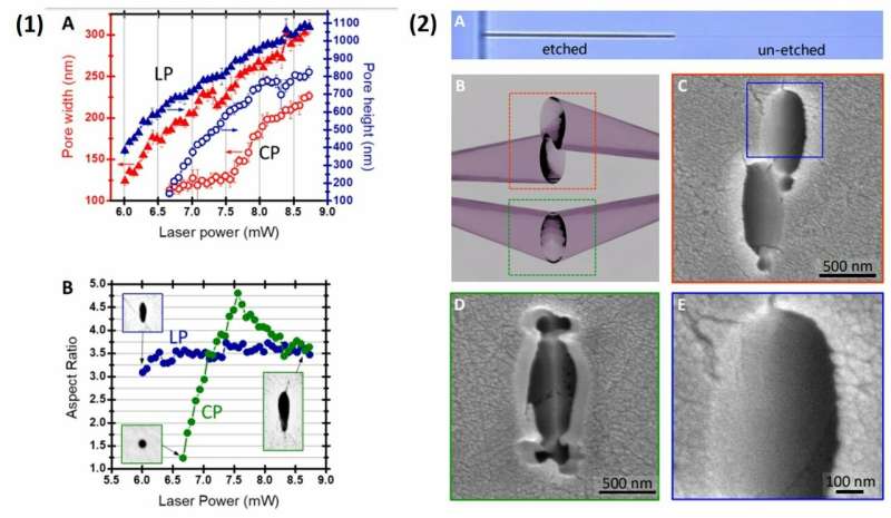
The scientists engineered the photonic structures using circular polarization to reproducibly create air pores in the nanoscale region below 200 nm. The nanophotonic structures (air pore photonic lattices) created in the crystal maintained spatial resolution equivalent to that obtained with state-of-the-art multiphoton polymerization lithography.
For practical applications, nanophotonic devices require robust and efficient optical interconnections to form large, complex circuit designs with other optical elements. To achieve this, Ródenas et al. controlled the differential etch rate to maintain large pore lengths between the photomodified volumes and the surrounding crystal. They used scanning electron microscopy (SEM) to observe and prove the 3-D etching process.
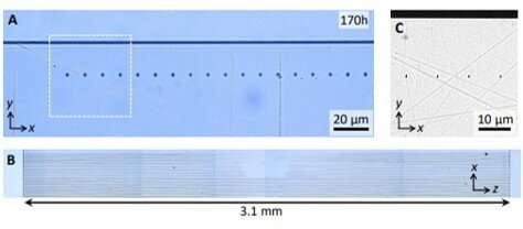
Within 170 hours, the scientists achieved nanopores with cross-sections of 368 x 726 nm2 and lengths of 3.1 mm; to show that nanopores with millimeter-scale length could be engineered in a single etching step. Nanophotonic devices typically require such lattice dimensions from the micrometric to the centimeter scale, without brittle fracture of the crystal due to excessive stress. In this way, the scientists implemented a scheme to homogenously etch nanostructures and microstructured optical waveguides (MOWs), on the desired scale across the whole sample.
To test if the observed selectivity of nanopore etching with YAG was transferrable to other crystal types, the scientists conducted similar experimental nanostructuring with sapphire. They found a parallel nanopore etch rate of ~1 x 10⁵ in sapphire, similar to YAG and higher than the rate previously observed with microchannels etched in sapphire. Ródenas and co-workers formed millimeter-long nanopores in sapphire with cross-sections as small as ~120 nm and tested the feasibility of the method by engineering nanopore lattices etched for 170 hours without fracturing the crystal.
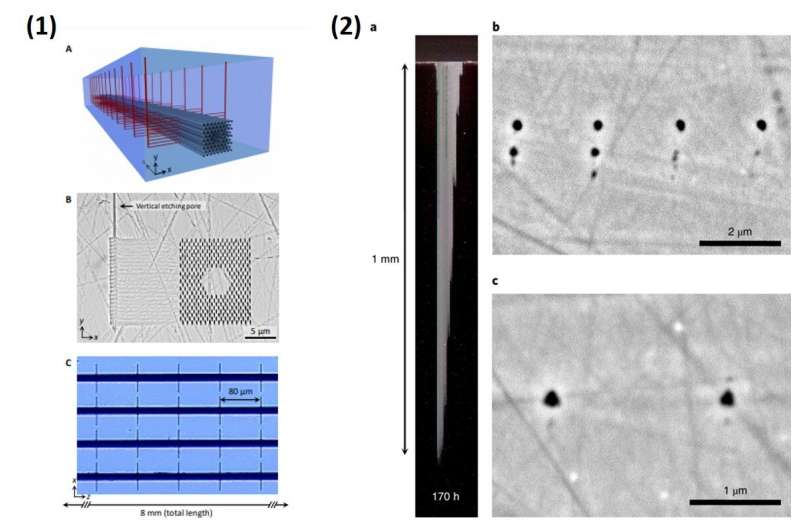
The capability to control lattice formation down to the nanometer scale will be useful in practical photonic applications. For instance, photonic bandgap lattices can be designed with stopbands in the visible to mid-infrared range in solid-state laser crystals for photonic information technology. To further expand the potential of the 3-D nanolithography technique, Ródenas et al. engineered MOW (microstructured optical waveguides) with different lattice spacings and cavity sizes. They obtained dimensions in the range of a centimeter in length, with 700 nm pitch grating observed under visible light illumination.
Ródenas et al. conducted theoretical and simulation methods of the subwavelength gratings prior to their material fabrication. For the numerical simulations, they used the finite element method (FEM) in COMSOL Multiphysics 4.2 software. The scientists used the same FEM software and method to model YAG MOWs prior to fabrication.
This ability to create controlled 3-D nanostructures of crystals opens up new routes to design compact, monolithic solid-state lasers. The resulting crystals can incorporate traditional cavity elements (gratings, fibres, microfluidic cooling channels) or novel microresonators inside the crystal. The prospect of engineering large, nanostructured laser crystals will provide a new basis for precision technology in metrological applications and allow for potentially new applications with ultra-strong deformable laser nanofibers in microelectronics and for drug delivery in medicine.
More information: Airán Ródenas et al. Three-dimensional femtosecond laser nanolithography of crystals, Nature Photonics (2018). DOI: 10.1038/s41566-018-0327-9
Markus Deubel et al. Direct laser writing of three-dimensional photonic-crystal templates for telecommunications, Nature Materials (2004). DOI: 10.1038/nmat1155
Amit Banerjee et al. Ultralarge elastic deformation of nanoscale diamond, Science (2018). DOI: 10.1126/science.aar4165
Journal information: Nature Photonics , Nature Materials , Science
© 2019 Science X Network


